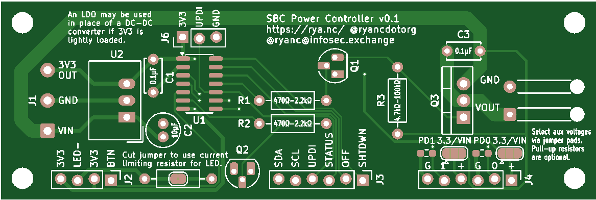
A top-down, 2D computer-generated view of a rectangular, green printed circuit board (PCB) design. The board features lighter green routing traces, exposed copper pads, and white silkscreen text and outlines detailing component placements. Silkscreen notes: Top center: "SBC Power Controller v0.1 https://rya.nc/ @ryancdotorg @ryanc@infosec.exchange" Top left: "An LDO may be used in place of a DC-DC converter if 3V3 is lightly loaded." Bottom left: "Cut jumper to use current limiting resistor for LED." Bottom right: "Select aux voltages via jumper pads. Pull-up resistors are optional." Footprints and pin labels: J1 Header: Pins for 3V3 OUT, GND, and VIN J2 Header: Pins for 3V3, LED-, 3V3, and BTN J3 Header: Pins for SDA, SCL, UPDI, STATUS, OFF, and SHTDWN J4 Header: Pins labeled G, 1, +, G, 0, + with jumper pads for PD1 3.3/VIN PD0 3.3/VIN J6 Header: Pins for 3V3, UPDI, and GND Integrated circuits: A 14-pin surface-mount footprint labeled U1 Transistors and regulators: 3-pin footprints labeled U2, Q1, Q2, and Q3 (with GND and VOUT labels nearby) Resistors: R1 and R2 (470Ω-2.2kΩ), and R3 (4.7kΩ-100kΩ) Capacitors: C1 (0.1μF), C2 (10μF), and C3 (0.1μF)
https://media.infosec.exchange/infosec.exchange/media_attachments/files/116/846/061/653/109/532/original/e841bb9df9b132ab.png